Attenuated oscilloscope probes
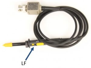
To minimize capacitive loading on the device under test, most probes use a x10 (also called 10:1) attenuator. This can often be adjusted, or compensated, to improve the frequency response. The following note explains the adjustment technique using two example probes with different adjustment arrangements. The instructions can be applied to any adjustable passive probe, although not all of the adjustments explained here may be required.
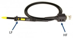 Figure 2: Another probe showing LF and HF trimmers
There are two types of compensation: low-frequency (LF) and high-frequency (HF). Some probes have only LF compensation, while others have both types. Pico oscilloscope probes are HF compensated at the factory and do not require adjustment but, if you wish to use a different probe with your PicoScope oscilloscope, you may need to adjust its HF compensation.
Low-frequency compensation
Low-frequency compensation (LFC) involves tweaking the frequency response of the x10 probe in the kHz region. LFC must be carried out before high-frequency compensation (HFC).

Figure 3: Scope probe model
Figure 3 shows a model of a typical probe. Cp is the stray capacitance of the probe tip itself. R1 is an in-series 9 MΩ resistor used to isolate the capacitance of the cable and input of the scope from the device under test. A consequence is the formation of a 10:1 attenuator with the 1 MΩ input impedance of the scope, Rscope.
Ccomp1 is a variable capacitor and forms the LFC tuning part of the probe. Cp serves to adjust and match the time constant of R1 and Ccomp1 to the time constant set by Cscope, Ccable and Rscope. In effect, we have a resistive divider at DC and a capacitive divider at high frequencies (above a few 100 kHz). Ccomp1 represents the trimmer at the top of the probe, close to the attenuation switch.
Ccomp2 and Rcomp represent the high-frequency compensation (HFC) part of the probe, to be discussed in the next section.
The easiest way to compensate the LFC part of a probe is to input a square wave with a relatively slow edge but, importantly, no overshoot.
Figure 4 shows how the waveform should look when LFC is correct. Too much and the High Frequency (HF) gain of the probe will be higher than its Low Frequency (LF) gain. With too little LFC, the HF gain will be lower than the LF gain.
 Figure 4: Low-frequency compensation
High-frequency compensation
Two variable factors affect the high-frequency response of the probe: the cable impedance, and the input impedance of the scope. The scope input is not usually a perfect capacitance, also having some series inductance and nonlinearity.
Figure 5 shows the typical characteristics of a ceramic chip capacitor used in a scope’s input. There is a dip in the impedance before it starts to increase again with frequency. This is due to the series inductance of the capacitor. The point of minimum impedance is called the resonant frequency and represents the frequency at which the inductive and capacitive impedances are equal.
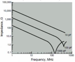
Figure 5: Characteristics of ceramic capacitors
This diagram gives some insight into how, at very high frequencies (VHF), the input of a scope is not quite as simple as a resistor in parallel with a capacitor, and this is further complicated by nonlinear characteristics of the PCB. The input impedance of high-frequency scopes consists of a 1 MΩ resistance to ground and a number of stray capacitances and inductances. Each of these has its own series and parallel inductive and capacitive components, and these often have a nonlinear characteristic at VHF, further complicating things.
To compensate for the nonlinearity, HF probes tend to shunt the input of a scope with a very small capacitor and a series resistor right at the BNC. This serves to move any nonlinearity into a higher frequency region, outside the intended range of the probe, without causing severe overshoot.
Rcomp and Ccomp2 represent the HF tuning components of the probe. This circuit is often on a PCB in a screened case right at the BNC connector to minimize the effects of the cable and noise pickup. A typical probe has two RC networks like this, each with its own adjustable resistor. One controls the mid-band frequencies and the other the high-band. Both should be adjusted until the correct response is obtained.

Figure 6: PicoScope 3206B pulse response without probe
To tune the HFC of a probe, a square wave with a very fast edge must be input into it. The waveform must have a fast edge (3x shorter rise time than the probe) with very little or no overshoot. At Pico we use a signal generator with less than 3% overshoot and a very fast rise time. Also the VSWR of the 50 Ω terminator used with the pulse generator should be considered, as a low-quality terminator can cause extra overshoot.
When tuning a probe, the pulse response of the scope should be observed first in order to match the probe response to that of the directly connected scope input. Figure 6 shows the pulse response of a PicoScope 3206B 200 MHz oscilloscope without a probe connected. The input pulse has a 250 ps rise time.
Note: The 200 mV range (2 V range in PicoScope with a x10 probe) must be used to tune the probes because it gives the best pulse response.
The slight overshoot and ringing occurs at approximately 1 GHz. This is mostly due to stray inductance of the PCB tracks leading into the first amplifier, as well as the amplifier itself causing some ringing.
Over-compensated and under-compensated pulse responses
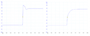
Figure 7: Over-compensated and under-compensated pulse responses of second probe
Figure 7 shows how over- and under-compensated pulse responses will look. The aim is to make the response as flat as possible. One should note the rise time when tuning a probe. For the PicoScope 3206B with TA131 probe, the rise time is approximately 1.4 ns. In Figure 7 the rise time of the under-compensated probe is of the order of 10 ns, giving a 40 MHz bandwidth. The rise time of the over-compensated probe is about 1.2 ns but the waveform is far from flat, giving an increasing gain in the 100 MHz to 300 MHz region.
Perfect compensation
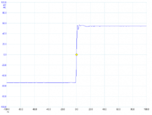
Figure 8: Perfect compensation
Figure 8 shows a perfectly compensated probe. Close inspection shows that the ringing and overshoot look similar to the directly connected pulse generator that we saw in Figure 6. The slight hump is desirable as it gives the probe and scope combination more bandwidth than the scope alone, without giving a lot of overshoot.
If you want to know more about oscilloscopes and other radio frequency products or data loggers, see our article Internet of Things.
Contact us


sales@logicbus.com | support@logicbus.com | 55-5431-6718 | Start conversation

