

Modbus RTU is a widely used protocol for industrial automation. It allows the exchange of information between master-slave devices. To do this, Modbus makes use of an addressing scheme which encompasses the data unit protocol or PDU and the logical address. In this blog we will explain how PDU data flows and the conversion between PDU addresses and logical addresses have been worked out.
Presentation of the Data Unit Protocol (PDU):
The PDU protocol is an essential part for data exchange between master and slave devices. this protocol is structured as follows:
Function (1 byte): serves as a command that tells the slave what action the master wants it to perform. It is a one-byte value that tells the device whether to read data, write data or request diagnostic information.
Register address (2 bytes): The register address field specifies the starting point of the register in the slave’s memory. This value provides the master with the location of the data to be manipulated or read. It is worth mentioning that Modbus defines the memory address of each data in a range between 0 and 65535.
Additional fields (up to 250 bytes): Depending on the action to be performed, this section can be up to 250 bytes long as it contains the instructions and information necessary to carry out an action. For example, when the action consists of reading data, this field will include the number of registers to be read, while when writing data the field would contain the values to be written to the device registers.

With these three blocks in the PDU protocol, Modbus RTU ensures an efficient and reliable flow of information between devices.
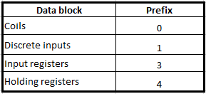
Modbus RTU defines 4 types of logic registers, each serving a specific purpose in industrial automation
- Coils (Discrete Outputs): Represents binary outputs that can be controlled by the master device . These have only two states 1 and 0. This type of registers are read and edited by the master allowing the control of industrial processes.
- Discrete inputs: They provide a binary data input to the master device. These registers are read only and usually represent the states of sensors and switches.
- Input registers: These registers store analog data that is captured by sensors. The registers are read-only by the master and provide it with information regarding the environment.
- Holding registers. These types of registers serve as two-way communication channels allowing read and write operations. They are used for slave device control and data storage.
Calculating the logical addresses of PDU addresses
In the Modbus protocol each data is assigned with an address between 0 to 65535. To convert PDU addresses to logical addresses such as: Coils, Discrete Inputs and Hold Registers. An offset is applied. The formula for such conversion is expressed as:
Logical address = Register address + Offset
ó
Register address = Logical address – Offset
The Offset values used may vary and are specific to the model and device used, so that an Offset value useful for one device will not work in other models. For this reason, manufacturers define the values to be used in the manual of each device in question.
For example, to reference data to a hold 14 register at a PDU address 12, a device manual might use the following representation. 4014 ó 400014. In each case, the first number, 4, indicates the hold registers. The choice between a 4XXX, 4XXXXX and 4XXXXX notation depends on the available memory space in the device: Thus, if all 65536 registers are in use, the 4XXXXX notation is used. If only a few registers are in use, the most common practice is to use the range 4001 to 4999.
The address of each register can be represented differently depending on the manufacturer, which can lead to some confusion. Here are some different possible representations:
- PDU address 13
- Logical address 4014 (here the offset is 4001)
- Logical address 40014 (here the offset is 40001)
- Logical address 400014 (here the offset is 400001)
Although the addresses defined by each manufacturer are different, the application of an Offset allows the PDU address to always be respected. For example:
- For logical address 4014 and offset 4001 -> PDU address = 4014-4001 = 13.
- For logic address 40014 and offset 40001 -> PDU address = 40014-40001 = 13
Thus, by using the offset, the protocol ensures that the PDU address is used consistently for all devices, regardless of the representation defined by the manufacturer.
The opposite can also occur in the input registers where the PDU address is 33. However, the SCADA software works with a 3XXXXXXXXXXXX format so the offset used in this case must take a value of 300001 for the input registers so that the PDU address is equal to 33.


sales@logicbus.com | support@logicbus.com | +1 619 616 7350 | Start conversation