

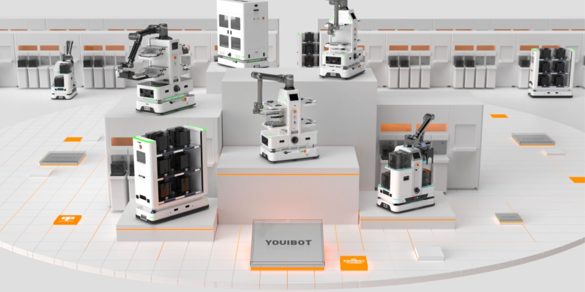
The semiconductor industry has always been driven by an relentless pursuit of higher efficiency, microscopic precision, and total automation. As semiconductor fabrication plants (fabs) continue to expand production capacity and process complexity, traditional material handling approaches are reaching their physical and operational limits.
Modern fabs require intralogistics infrastructure that goes beyond simple point-to-point transportation. Today’s manufacturing environment demands systems that adapt dynamically to shifting production schedules, interact natively with fab-wide enterprise software, and support real-time intelligent decision-making.
This paradigm shift is accelerating the adoption of embodied intelligence technologies—specifically mobile manipulation robots (AMRs equipped with collaborative robotic arms). By fusing autonomous mobility with high-precision robotic handling, these platforms create a far more flexible, scalable, and resilient material flow ecosystem.
Beyond Traditional AMHS: The Need for Greater Flexibility
Automated Material Handling Systems (AMHS), particularly Overhead Hoist Transport (OHT) networks, have long served as the primary backbone of semiconductor fab logistics.
While OHT systems excel at delivering high throughput across fixed, high-volume production routes, they present clear operational limitations when fabs require:
-
Rapid line layout reconfigurations.
-
Process expansions without prolonged facility downtime.
-
Tactical, flexible handling for small-batch runs, test wafers, or localized equipment maintenance.
To address these challenges, leading semiconductor manufacturers are deploying mobile manipulation robots to complement existing AMHS infrastructure. This hybrid approach delivers autonomous transportation combined with automated loading and unloading directly at the tool level—all within a single, self-contained mobile platform.
Precision, Stability, and Cleanroom Compatibility
Wafer fabrication tolerates zero margin for error. Transporting delicate silicon wafers demands extreme mechanical stability, zero particle contamination, and millimeter-level alignment at the tool load port.
To meet these uncompromising standards, Youibot’s semiconductor mobile manipulation solutions are engineered specifically for high-cleanroom fab environments, delivering industry-leading performance metrics:
  Positioning Accuracy: Up to ±2 mm
  Transportation Vibration: Ultra-low ≤ 0.1g
  Cleanroom Rating: ISO Class 3 Certified
  Safety Architecture: 360° Multi-Sensor Fusion
  Transfer Cycle Time (OW12-300 / OW8-350): ~25 seconds
Key Engineering Highlights:
-
±2 mm Positioning Accuracy: Ensures flawless physical alignment with tool load ports, stockers, and automated material stations.
-
Ultra-Low Vibration (≤ 0.1g): Eliminates mechanical shock during movement, preventing wafer micro-cracking or displacement inside FOUPs.
-
ISO Class 3 Cleanroom Certification: Utilizes sealed, non-particle-generating materials designed for sub-micron fabrication environments.
-
360° Safety Protection: Combines LiDAR, 3D vision cameras, and tactile bumpers for safe, continuous co-existence with fab personnel.
-
Rapid Transfer Cycles: The OW12-300 and OW8-350 mobile manipulators complete material exchange cycles in as fast as 25 seconds, delivering throughput comparable to traditional AMHS while retaining total routing freedom.
Intelligent Fleet Coordination at Scale
As fabs deploy dozens or even hundreds of autonomous mobile manipulators, centralized fleet management becomes the single most critical factor in maintaining high overall equipment effectiveness (OEE).
Modern fleet scheduling platforms continuously analyze:
-
Real-time material demand fluctuations across processing bays.
-
Individual tool operational statuses and queue lengths.
-
Traffic density and aisle congestion in real time.
-
Dynamic job priorities and batch routing requirements.
-
Battery state-of-charge and automated charging windows.
By intelligently coordinating large, heterogeneous fleets simultaneously, the system dynamically recalculates routes in milliseconds—eliminating transport bottlenecks and maximizing tool utilization rates even during complex manufacturing shifts.
Creating a Closed-Loop Information Flow
True automation extends far beyond physical transport; it requires complete synchronicity between the physical flow of goods and the digital flow of data.
Mobile manipulation robots integrate directly into the fab’s digital infrastructure, communicating seamlessly with:
-
MES (Manufacturing Execution Systems)
-
MCS (Material Control Systems)
-
WMS (Warehouse Management Systems)
-
Automated Stockers and wafer storage pods.
-
Smart Building Infrastructure: Autonomous elevators, automatic doors, and cleanroom airlocks.
By connecting mobile manipulation hardware directly into the factory control loop, plant managers gain end-to-end visibility and complete lot traceability. From initial ingot processing to final wafer probing and packaging, every physical movement is tracked, recorded, and optimized automatically.
Supporting the Entire Semiconductor Value Chain
The operational scope of mobile manipulation robots spans every major stage of microelectronics manufacturing:
| Manufacturing Phase | Target Materials & Carriers |
| Front-End Wafer Fabrication | Large-diameter silicon wafers, FOUPs, and FOSBs. |
| Photolithography | High-value Photomask reticle boxes and pods. |
| 3rd-Gen Semiconductors | Silicon Carbide (SiC) and Gallium Nitride (GaN) substrates. |
| Back-End Packaging | Leadframes, substrate carriers, and advanced packaging materials. |
| Testing & Quality Control | Test trays, probe cards, and specialized inspection carriers. |
Technical Overview: Youibot OW12-300 & OW8-350
| Parameter / Feature | Specification Overview |
| Target Models | Youibot OW12-300 / Youibot OW8-350 |
| Repeatability Precision | Up to ±2 mm |
| Max Transportation Vibration | ≤ 0.1g |
| Cleanroom Standard | ISO Class 3 Certified |
| Material Exchange Time | As fast as 25 seconds |
| Navigation Mechanism | Markerless Laser SLAM |
| Protocol Compliance | SEMI standards compliant, open MCS / MES / WMS APIs |
The Future of Semiconductor Logistics
The future of fab automation is not simply about moving materials faster—it is about establishing intelligent, self-aware logistics nodes capable of perceiving their environment, collaborating with enterprise software, and executing real-time decisions.
By uniting autonomous mobility, robotic manipulation, intelligent fleet coordination, and deep protocol integration, mobile manipulation robots empower semiconductor manufacturers to build more agile, scalable, and resilient production environments.
Partner with Logicbus for Advanced Industrial Robotics
At Logicbus, we provide cutting-edge industrial automation, connectivity, and autonomous mobile robotics solutions for high-tech manufacturing and semiconductor facilities across the United States.
Whether you are looking to optimize material transport, integrate cleanroom-grade AMRs, or connect mobile fleets to your existing MES/WMS architecture, our application engineering team is ready to assist.
-
Consult with a Logicbus automation engineer to evaluate your intralogistics workflows.
-
Explore our full portfolio of industrial mobile robotics, sensors, and network gateways.
Contact Logicbus Today to Learn More




sales@logicbus.com | support@logicbus.com | +1 619 616 7350 | Start conversation